The photomask inspection market plays a vital role in the semiconductor manufacturing ecosystem, ensuring that photomasks—the templates used to print circuits onto wafers—are free from defects that could compromise chip performance. As chip designs become increasingly complex and smaller process nodes dominate the industry, photomask inspection tools must evolve rapidly. However, despite their growing necessity, several hindrances are slowing the widespread adoption and advancement of photomask inspection technologies globally.
High Cost of Advanced Inspection Systems
One of the most pressing challenges in the photomask inspection market is the prohibitively high cost associated with advanced inspection equipment. Systems capable of detecting minute defects at nanometer scales—especially those compatible with EUV lithography—require sophisticated optical and electron beam technologies. These tools can cost tens of millions of dollars, making them inaccessible to smaller fabs and niche manufacturers.
The cost burden is further compounded by the need for regular calibration, maintenance, and upgrades. As a result, even large semiconductor players must carefully balance their capital expenditures, often leading to delays in acquiring or upgrading photomask inspection systems.
Limited EUV Lithography Compatibility
With the industry shifting toward extreme ultraviolet (EUV) lithography for sub-7nm and 5nm nodes, inspection technologies must be capable of handling the unique challenges posed by EUV masks. These include multilayer reflective structures and the potential for phase defects that are not easily detectable using traditional optical methods.
Unfortunately, EUV-compatible inspection tools are still in the early stages of development and commercialization. Actinic inspection, which uses EUV light for defect detection, remains technologically complex and expensive. The limited availability and slow rollout of actinic inspection systems hinder the industry's ability to scale EUV production efficiently.
Technological Complexity and Skill Gaps
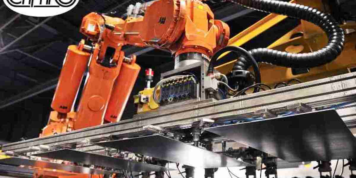
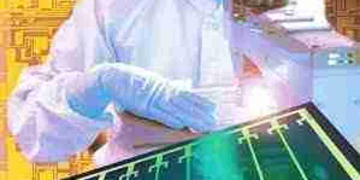
Modern photomask inspection tools incorporate a wide range of technologies, including optical inspection, e-beam systems, AI-based analytics, and deep learning algorithms. While these innovations are essential for accurate defect detection and classification, they introduce a high level of complexity into both operation and maintenance.
This complexity demands a skilled workforce, including data scientists, engineers, and technicians trained in both hardware and software systems. However, there's a noticeable shortage of skilled professionals globally, particularly in emerging semiconductor markets. The talent gap makes it challenging for fabs to fully utilize advanced inspection systems and achieve optimal return on investment.
Lengthy Validation and Integration Time
Photomask inspection systems must undergo rigorous validation processes before being deployed in high-volume manufacturing. These validation phases are critical to ensure defect detection accuracy, system stability, and compatibility with fab workflows. However, they can take months to complete and often delay the implementation of new tools.
Furthermore, integrating new inspection technologies into existing production lines can be disruptive, requiring adjustments to other equipment, retraining of personnel, and calibration of process parameters. These time-consuming processes discourage frequent upgrades and slow the pace of innovation adoption across the industry.
Lack of Standardization in Defect Classification
As chip designs evolve and new defect types emerge, there's a growing need for standardized defect classification systems. However, the industry lacks a universal framework for defining and categorizing photomask defects, especially for EUV masks and advanced packaging formats.
This lack of standardization leads to inconsistencies in inspection results, making it harder for manufacturers to compare tool performance or share data across fabs. It also complicates the implementation of automated defect classification systems, which rely on consistent labeling and categorization to function effectively.
Pressure on Smaller and Regional Players
While major players in the photomask inspection market have the resources to invest in advanced R&D and tool development, smaller and regional equipment manufacturers struggle to keep pace. These companies often face limitations in funding, access to cutting-edge technology, and opportunities for collaboration with leading fabs.
As a result, the market becomes increasingly consolidated, with a few dominant players controlling most of the innovation. This concentration reduces competitive diversity and slows the emergence of cost-effective alternatives and localized solutions in developing markets.
Data Management and Cybersecurity Concerns
Photomask inspection generates vast amounts of high-resolution image data and process control information. Managing this data requires robust data storage, transfer, and analysis infrastructures. As fabs transition to cloud-connected platforms and smart manufacturing ecosystems, the risk of cybersecurity threats also increases.
Protecting intellectual property and maintaining data integrity are critical challenges that require continuous investment in cybersecurity solutions and protocols. These concerns add an additional layer of complexity and cost to the deployment of advanced inspection systems.
Conclusion: Navigating the Roadblocks Ahead
Despite its critical role in semiconductor manufacturing, the photomask inspection market is hindered by a complex set of challenges that affect cost, scalability, and technological integration. From high capital requirements to EUV compatibility issues and skill shortages, these hindrances must be addressed strategically for the market to grow sustainably.
Future progress will depend on collaborative efforts among equipment makers, fabs, research institutions, and governments. By tackling these roadblocks head-on—through standardization, skill development, cost optimization, and R&D support—the industry can ensure that photomask inspection keeps pace with the rapid evolution of semiconductor technology.